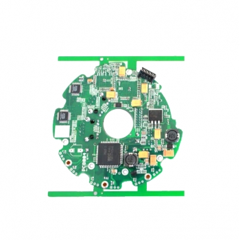
PCB or printed circuit boards have brought a revolution towards the electronic marketplace. PCB fabrication may be separated into the PCB board’s manufacturing approach. A PC board should really be such that it fits to the provided area with supporting total performance. Nonetheless, utilizing the prototype is actually a sophisticated endeavor that calls for awareness and cautious application.
Subsequent, heat the board till the solder paste melts (reflows) doing work using a heat gun, a toaster, or an oven. Right here too ink is utilized, whilst the method varies a little. From there, you are able to locate not less than 3 (three) conductive layers in only one multilayer board. For those who have ever had the opportunity to look within gadgets such being a television as well as electronic video games, you are going to recognize these green colored boards with an intricate network of copper wires operating throughout the surface.
This process ascertains regardless of whether a advised PCB layout will execute as anticipated thereby revealing any possible flaws and so enabling the designers for making any vital alterations. In order to find a credible organization which will kind out all problem inside of short span of time, you may utilize the world-wide-web and make some exploration that takes only handful of minutes. Though, substantial volume manufacturing is executed by machine placement. The latest electronic devices usually need much more focus in order that the PCBs can run appropriately, which means the PCBs are produced by hand rather than as a result of a mass production approach.
It will be actually good to stick to these actions. Data is surely an instant match and proposed in regards to industrial gadgets and gadgets. So as to design these boards, suitable capabilities and expertise is required. There are various distinctive kinds of electrical printed circuit board during the market place lately.
Around the hand, complex PCB testing demands to become performed in good detail, specially in case of surface mount technological innovation (SMT). Traces among gadgets had been created with self-adhesive tape. Up to twelve this kind of layers may be simply accomplished while manufacturing a PCB. Every individual is acquainted using the PCB prototyping and has practical experience functioning with a number of component program forums.view website